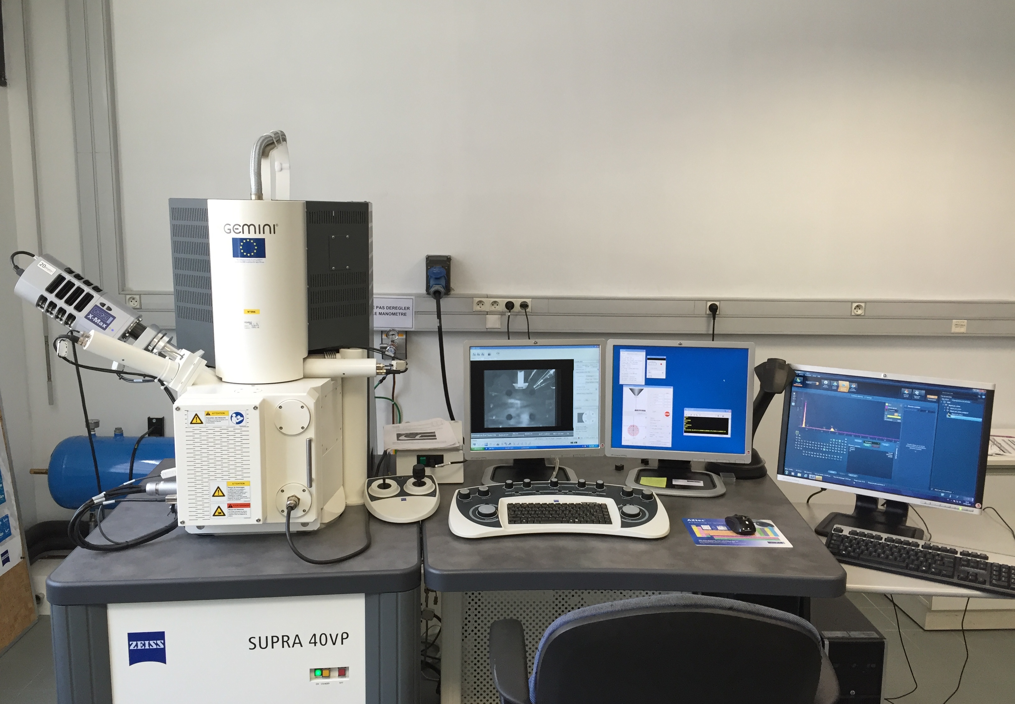
Scanning Electron Microscopy (ZEISS-supra 40 vp/gemini column)
Scanning Electron Microscope (SEM) scan a sample with a focused electron beam and deliver images with information about the sample’s morphology and composition.
Our microscope is equipped with several detectors: Secondary and Backscattered electron detectors, an In-lens electron detector, a Secondary electron detector for environmental conditions and an Oxford Energy-dispersive X-ray Spectroscopy (EDS). It operates in both high vacuum and variable pressure modes with a high resolution.
The analysis can be done on solid materials having a resistance to incident electron beam (< 30 kV). Examples: Metal, composite, polymer and biopolymer, coating, fibers …
Investigations:
– Microstructure characterization of materials and detection of surface fractures
– Analysis of morphology and chemical composition of samples
– Cross section microscopy (coatings, composite materials …)
– Simultaneous SEM and EDS mapping collected from the same surface area
– Detection of surface contamination, dimensional analysis and particle identification
For sample preparation, sputter coater system (carbon and gold metal) and polishing machine (for cross section analysis) are available in the lab.


